
Wafer dicing, scribing & grooving
UV/green DPSS laser processing of Si, SiC, sapphire.
Eksma Optics offers
- High LIDT and low absorption coatings for laser optics operating at 220-400 nm ranges
Laser processing sits at the heart of semiconductor manufacturing — wafer dicing, stealth dicing, excimer annealing and inspection systems all depend on UV and DUV optics that hold their performance under continuous industrial duty. At 355 nm and below, coating absorption and damage threshold decide tool uptime.
Eksma Optics supplies high-LIDT UV optics, F-theta and beam delivery lenses, and LBO / CLBO harmonic crystals for semiconductor laser tools — with low-absorption coatings from 190 nm and full in-house metrology for lot-to-lot traceability. We offer flexible production, from custom engineering samples to dedicated OEM lines for tool builders.
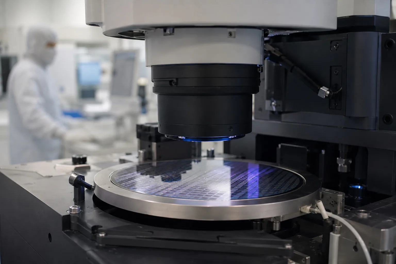
Optics, coatings, crystals and assemblies engineered for each semiconductor application — to your spec, from prototype to volume.
UV/green DPSS laser processing of Si, SiC, sapphire.
Eksma Optics offers
Sub-surface IR (1064 nm) modification of silicon wafers.
Eksma Optics offers
Defect detection, overlay and CD measurement systems.
Eksma Optics offers
DUV line-beam systems for LTPS display and semiconductor annealing.
Eksma Optics offers
Microvia drilling, TSV, wafer-level marking.
Eksma Optics offers
We are actively seeking strategic partnerships to invest and expand our manufacturing capacity — creating dedicated production lines of optical components and assemblies for your tailor-made semiconductor solutions.
Expert team: 10+ seasoned scientists, each with a decade-plus of experience.
End-to-end traceability with full control from raw materials to final testing.
Multi-stage quality assurance with stringent procedures for reliability.
Accreditations and certifications that let partners qualify us quickly.
Leverage our 40+ years of photonics expertise for your semiconductor applications — from R&D prototypes to high-volume production.
Contact us